SCALING AI SUSTAINABLY: HOW 300 MM GAN WAFERS ARE REVOLUTIONIZING THE DATA CENTE
The rapid expansion of artificial intelligence is pushing data center energy demands to unprecedented levels. To sustain this growth, the computing industry is shifting away from traditional silicon toward Gallium Nitride (GaN). This high-performance semiconductor material is a game-changer for power density, offering superior efficiency, faster switching speeds, and better thermal management.
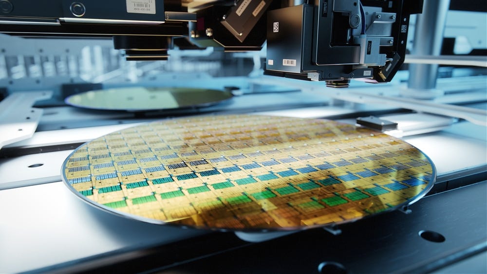
The real breakthrough, however, lies in the transition from 200 mm to 300 mm wafers. This move to a larger scale isn’t just about size; it’s about economic and technical viability. Larger wafers provide roughly 2.3 times more chips per unit, significantly lowering production costs and bringing GaN closer to cost parity with silicon. Furthermore, 300 mm manufacturing allows for more precise process control, resulting in enhanced device performance.
By integrating 300 mm GaN into server power supplies and voltage regulators, data centers can substantially reduce energy consumption and physical footprints. This evolution is essential for scaling AI workloads sustainably, ensuring that the infrastructure powering the next generation of innovation is as efficient as the algorithms it runs.
"As a silicon alternative, GaN really shines when high power and high efficiency are needed... The shift to 300mm may be driven by the immediate demands of AI, but over time it can pave the way for innovations we haven't yet imagined."
Author: David Haynes, Vice President of Specialty Technologies
Source: Power Electronics News